We shall exhibit at "nano micro Biz"
Mar. 19, 2015
We shall exhibit at "Nano Micro Biz", which will be held between the 22nd -24th of April.
Here are the details.
Details
| Date | 22nd(Wed) to 24th(Fri) of April |
|---|---|
| Venue | Pacifico Yokohama |
| Booth NO |
D-15 |
Contents
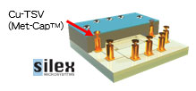
MEMS volume production foundry Co-exhibitor : Silex microsystems
- φ6",8" compatible MEMS foundry
- Unique TSV technology : Sil-Via
(For better thermal resistivity and higher density by applying all Si structure) - Unique TSV technology :Met-Via / Met-Cap
(For better yield by applying Cu hollow structure) - Unique implementation methodology : SmartBLOCK
A methodology to reduce time and cost by applying proprietary process library and short loop confirmation)
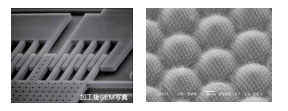
Nano / micro fabrication services
We offer nano/ micro fabrication service using the process of nanoimprint or semiconductor /MEMS.
Please consult us if you consider creating nano/ micro-scale sample or evaluation
[ Examples of manufacturing process ]
- Thin film deposition (Sputtering, Evaporation, CVD, ALD, Electroplating, etc.)
- Photolithography (Aligner, Stepper, E-Beam etc.)
- Etching (Wet, Dry, Deep etching for high aspect ratio pattern (ICP), etc.)
- CMP (Metal, Oxide film, Nitride film etc.)
- Wafer bonding (Room temperature bonding, Plasma bonding, Eutectic bonding, Anodic bonding, etc.)
- Nanoimprint (Mold fabrication, Imprint service, Anti-sticking coating etc.)
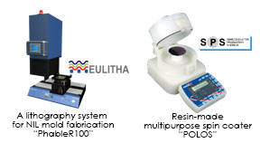
MEMS development tools
- A lithography system for NIL mold fabrication “PhableR 100”
- Resin-made multipurpose spin coater “POLOS”
Made from chemical resistance resin. The system is applicable to multiple processes (coating, etching, development, cleaning, drying) - “AML wafer bonder”
Alignment and bonding can be done in a single chamber. - “OAI Model 800” mask aligner
Using OAI’s high quality light source, it is a compact mask aligner which is suitable for R&D Also, various UV meters and proves are available.
If you intend to visit the event, do not hesitate to stop by our booth.