We shall exhibit at "SEMICON Japan 2015"
Nov. 20, 2015
We shall exhibit at "SEMICON Japan 2015" which will be held at Tokyo Big Sight during 16th(Wed) to 18th(Fri) of December, 2015.
Details are as follows.
Details
| Date & Time | 16th (Wed.) to 18th(Fri.) of December, 2015 10:00−17:00 |
|---|---|
| Venue | Tokyo Big Sight |
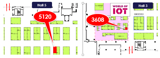
| Booth NO |
Hall 5/ 5120, Hall2 / 3608 |
Contents
Hall 5 / 5210
We offer optimal solution for various issues such in thin film deposition, bonding & sputtering target and consumable parts for semiconductor manufacturing equipment which customers face in development to mass production stage.
"Thin film fabrication services"
- Thin film deposition process
- Sputtering、CVD、Vapor deposition
- Photolithography, Etching
- Contact aligner, Stepper, Electron beam lithography
- Dry/Wet etching
- Nanoimprinting total solution
- Mold fabrication〜imprint services (From initial trial to mass production)
- CMP/ Wafer bonding services
"Bonding process and sputtering target sales"
- Bonding process for cylindrical target (AZO for touch panel, SC and Carbon for battery)
- Specialized target for R&D purpose such as CZC for metal mesh application
"Consumable parts and maintenance parts for semiconductor manufacturing equipment"
- High functional parts for CMP process (retainer ring, upgrade parts for wet cleaning equipment)
- Repair services for Ion implantation process equipment
- Sputtering/ Etching process Dual HDD Full compatible compact flash for FDD
Hall 3 / 3608
Development for innovative products and services for our life and environment have been progressing by the spread of IoT technology.We offer distinguishing processing technologies which is applicable for IoT related devices in "Environment・Energy" "Wearable・Medical"
"High resolution process by Nanoimprint technology"
- Enlarge surface area in fuel sell
- Increase efficiency of solar battery
"Thin film deposition by sputter process"
- Inhibitory layer for metal allergy (Ti)
- Optical catalysis layer(TiO2)
"R t R thin film deposition"
- Human sensor
- Wearable devices
"MEMS device development and fabrication by dedicated MEMS processing technology."
- Energy harvest by Piezo electric device
- “Intelligent nose ring” which is nose ring form thermometer for animal husbandry
"Global network to support Intellectual Property"
If you intend to visit the event, do not hesitate to stop by our booth.