We shall exhibit at "nano tech 2016"
Jan. 6, 2016
We shall exhibit at "nano tech 2016 - The15th International Nanotechnology Exhibition & Conference" which will be held at Tokyo Big Sight during 27th (Wed) to 29th (Fri) of January, 2016.
Details are follows.
Details
| Date | Jan.27(Wed.) -Jan.29(Fri.), 2016 |
|---|---|
| Venue | Tokyo Big Sight |
| Booth NO |
4E25 |
Contents
We realize High Added-Values in various growth fields such as IoT, Medical Care and Environment by Thin Film Technologies.
Saving Energy、Environmental Issue、Medical Treatment /Medical Care
[Application] Solar cell, Battery, Wearable, Sensor, Micro needle
- Thin film deposition services:semiconductor / LCD, power device, protective film, material development etc.
- Etching process services:Patterning /Etching process services、Dry / Wet etching
- MEMS Total Support
Design support from technological strategy -- design -- simulation
Prototyping based on design such as prototyping -- pilot production --
Capable for expansion to mass production
Functional Material, Biomimetic
[Application] Photo catalyst, Photonic crystal
- Nanoimprint / Mold fabrication for soft lithography Trial mold for initial evaluation(Anti-reflection、Micro lens etc.)
- Imprint services(Thermal /UV imprint、Injection molding)
- Original anti-sticking treatment(Fine MoZt)
- Mold cleaning services / Mold replication services

Life Sciences
[Application] DDS, Bio sensor
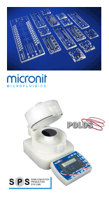
- Micronit Microfluidics:Manufacturing glass-made microfluidic chips applied to micro and nano technologies. Provided with Basic experiment, Custom design, Microfluidic related equipments.
Microfabrication Equipment
- SPS Europe:The versatile, all plastic single substrate spin processors specifically designed for applications for spin developing, spin etching, rinse / cleaning, spin drying with high resistivity for chemical and contamination.
If you intend to visit the event, do not hesitate to stop by our booth.