Silex Microsystems:MEMS foundry services (support documentation)
Foundry capability
Lithography
| 6 inch | 8 inch | |
|---|---|---|
| Contact 1:1 Aligner | Front/Back side | Front/Back side |
| Alignment Accuracy | ∼1µm, front side | ∼1µm, front side |
| ∼2µm, back side | ∼2µm, back side | |
| Minimum Features | ∼0.8µm, vacuum mode | ∼0.8µm, vacuum mode |
| ∼3µm, proximity mode | ∼3µm, proximity mode | |
| Stepper 5:1 Aligner | Front side | Front/Back side |
| Alignment Accuracy | ∼0.1µm | ∼0.1µm, Front side |
| - | ∼0.3µm, Back side | |
| Minimum Features | ∼0.5µm | ∼0.35µm |
| Resist Thicknesses | 1∼10µm, >20µm Positive | 1∼10µm Positive |
| 1∼10µm, >20µm Negative | 1∼10µm Negative | |
| BCB | available | - |
| Lift-Off | available | - |
| Spray Coating | available | - |
Plasma Etching
| 6 inch | 8 inch | |
|---|---|---|
| DRIE | available | available |
| Dielectric Etching (SiO2, SiN, etc.) | available | available |
| Polysilicon Etching | available | available |
| Polymer Etching and Stripping | - | available |
| Metals | Al, AlCu, TiW | TiN, AlCu |
| Oxide ICP | available | - |
Plasma Deposition
| 6 inch | 8 inch | |
|---|---|---|
| PECVD Oxide | available | available |
| PECVD Nitride | available | available |
| PECVD TEOS | - | available |
| SACVD Oxide | - | available |
Wafer Bonding
| 6 inch | 8 inch | |
|---|---|---|
| Silicon Fusion Bonding | available | available |
| Au-Si, Au-Sn Eutectic Bonding | available | available |
| Anodic Bondin | available | available |
| Thermo-compression Bonding | available | available |
| Adhesive Bonding | available | available |
| Alignment Accuracy: Wafer Pairs | <5um | <3um |
| Alignment Accuracy: Multi-wafer Stacks | <5um | <3um |
| DI Wafer Clean (Megasonic; Brush) | available | available |
| Controlled Ambient or Vacuum | available | available |
Back End
| 6 inch | 8 inch | |
|---|---|---|
| Automated Dicing | available | available |
| Au and Al Wire Bonding | available | available |
| Lapping for Wafer Thinning and Polishing | available | available |
| Epoxy and Solder Die Attach | available | available |
Furnace Process
| 6 inch | 8 inch | |
|---|---|---|
| Thermal Oxidations (900-1050℃) | Wet/Dry/Mixed | Wet/Dry/Mixed |
| Annealing Processes (densification, bond or forming gas) |
available | available |
| Vacuum Anneal | available | - |
| Metal Sintering | available | available |
| RTP | available | available |
| Doping Processes Z (ion implantation, POCI) |
available | available |
| LPCVD nitride (standard, low stress) | - | available |
| Ant-Reflective Coatings | available | - |
| LPCVD oxides (LTO, PSG, TEOS) | available | available |
| LPCVD Silicon | Amorphous, Poly, Fine-Grain Poly | Amorphous, Poly (in-situ P-doped poly coming) |
Wet Etching
| 6 inch | 8 inch | |
|---|---|---|
| Anisotropic silicon etching (KOH, TMAH) | available | - |
| Wet etching of dielectrics (i.e. different oxides and nitrides) |
available | - |
| Vapour HF | available | - |
| Wet cleaning process (acid and solvent based) |
- | available |
| Fully-automated Spin Solvent | - | available |
Metalization
| 6 inch | 8 inch | |
|---|---|---|
| Sputter Deposition | Al, Au, Cr, Cu, Ti, TiW, AlCu | Ti/TiN, Cu, W, AlN, Mo, AlCu |
| Evaporation | Au, Cr, Ni, Pt, Si, Sn, Ti | - |
| Electroplating | Au, Sn | Ni, Au, Cu, Sn Integrated Seed Layer Etch |
| Electroless Plating | Au, Ni | - |
Metrology
| 6 inich | 8 inch | |
|---|---|---|
| SEM with CD-Tool | available | available |
| Ellipsometer | available | available |
| Interferometer | available | available |
| Inspection Microscopes | available | available |
| CD Microscopes | available | available |
| White Light Interferometer | available | available |
| Surface Profiler | available | available |
| Film Stress Measurement | available | available |
| Sheet Resistance (4-point probe) | available | available |
| Surfscan | available | available |
| XRD | available | available |
Testing
| 6 inch | 8 inch | |
|---|---|---|
| Automated Probing | available | available |
| Automated Electrical Parametric Testing |
|
available |
| Customer-specific Test Rig | available | available |
| Test Development (Prototyping and Volume Production) |
available | available |
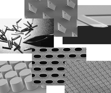
Expertise in MEMS devices
- Acceleration sensor
- Gyro
- Pressure sensor
- Cantilever
- Touch Membrane
- Flow sensor
- Filter structure
- CMOS interposer
- Needle structure
- IR sensor
- Cell analysis device
- Microphone
- RF switch
- Lab-on-a-chip
- Printer head
- Drug delivery
- Mirror structure
- Optical bench
- Micro pump