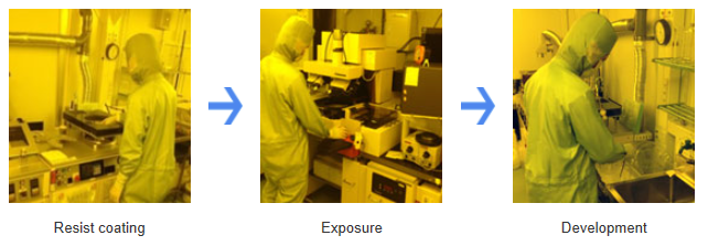
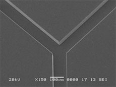
The semiconductor photolithography/etching fabrication service offered by Kyodo International decreases the R&D costs, lessens the burden of fabrication and increases the development speed for our customers.
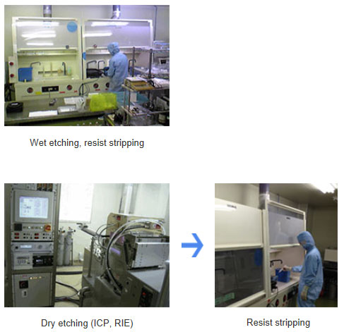
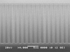
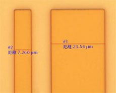
We use wet etching, ion milling, RIE etching among many other technologies in order to answer your manufacturing requests about circuit patterning, test patterning, improvement of the surface conditions, test evaluation, process conditions control, etc. Nowadays, in order to perform the needed processes for deep etching and nanoimprint mold manufacturing, we currently employ our ICP and D-RIE technologies. Furthermore, in addition to thin film formation and etching, we offer a wide range of micro-technology processes such as exposure, ashing among others.