Backside electrodes for Power devices (Al, Ti, Ni, Au, Ag)
Backside electrode deposition for Power devices with no chipping at dicing
We offer contract manufacturing of backside electrode for power device such as up-to-date IGBT or Diode.
Features
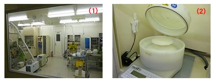
- Operation in clean room (Class 1000) [Pic(1)]
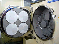
- Natural oxide removal by DHF (right before sputtering) [Pic(2)]
- Realize good adhesion to prevent chipping at dicing
- Available for thin wafer (expertise in t=100µm)
Major structures
- Ti-Ni-Au
- Ti-Ni-Ag
- Al-1%Si etc.
Suitable for customers such as;
- Thin film with better adhesion for backside electrode.
- Evaluate various film structure or thickness for backside electrode.
- Looking for facility to realize small volume production of backside electrode.
DHF cleaning test (Si φ8”)
HF cleaning procedure
1. Verify no damages to wafer caused by chuck
2. Control chemical contamination of back side
3. Confirm cleaning by HF
1. Verify no damages to wafer caused by chuck
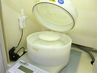
| Equipment | Polos MCD300 [picture] |
|---|---|
| Chuck type | Dedicated chuck for thin film wafer |
| Control wafer thickness | 625µm, 165µm, 100µm |
Results: In all three wafers no damages were observed.
2. Contamination of wafer back side
| Method | While spinning drops of ultra-pure water are dispensed on the wafer. After operation the back side is checked for water droplets. |
|---|---|
| Spin conditions | A) Ultra-pure water: Employed our companies cleaning conditions, followed by back side inspection. B) DHF: Employed our companies cleaning conditions, followed by back side inspection. |
Results A, B and A+B: In all cases no back side contamination is observed.
*Also true for thicker wafer.
3. Confirmation of cleaning by HF
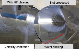
| Method | After HF treatment the wafer is sprayed with ultra-pure water. The hydrophobic state of the surface is checked. |
|---|---|
| Wafer thickness | 100µm and 165µm |
Results:HF treated surface = hydrophobic, non HF treated surface = hydrophilic
4. Measurement of removal of oxide film
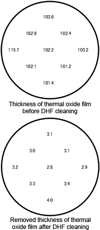
| Test wafer | ・φ8"Si ・About 100nm thermal oxide ・One sided polish |
|---|---|
| Removal conditions | Proprietary |
| Natural oxide film etching rate | ・Average etching rate 3.2 nm/30 sec ・Maximum rate 4.0 nm/30 sec (edge) ・Minimum rate 2.8 nm/30 sec (cente) |
Results: General native oxide thickness 2.4nm, lowest etching rate 2.8nm/30sec
removal of thermal natural oxide film is possible
検索用入力欄
記入時注意事項
- テーブルの行列は変更しないでください。
- 分類が複数ある場合は、| ←半角の縦棒で区切って連続で入力してください。
また、区切り文字の前後に空白は入れないでください。
| 製品分類1 | Deposition, Photolithography, Etching |
|---|---|
| 製品分類2 | Backside electrode |
| プロセス分類 | Prptotyping, R&D |
| サムネイル画像 |  |
| 説明文 |
|
| リダイレクトURL |
|